


Flip Chip Packaging Substrate Manufacturing
Posted by PCB123
from the Technology category at
24 May 2023 04:26:33 pm.
Share this page: 


Flip chip packaging has revolutionized the field of microelectronics, transforming the design and production of electronic devices. At the core of this technology lies the flip chip packaging substrate, a vital component facilitating electrical and mechanical connections between the integrated circuit (IC) and the package. This article explores the concept of flip chip packaging substrates, delves into recent advancements, and highlights their broad range of applications. Understanding Flip Chip Packaging Flip chip packaging involves directly mounting the IC face-down onto the substrate or carrier, contrasting traditional methods like wire bonding. Instead of wire bonds, flip chip packaging utilizes solder bumps or balls to establish electrical connections between the IC’s bond pads and corresponding pads on the substrate. This approach offers several advantages, including improved electrical performance, reduced interconnection lengths, efficient thermal dissipation, and increased input/output (I/O) density. The Role of Flip Chip Packaging Substrates Flip chip packaging substrates serve as the foundation for assembling flip chip packages, providing crucial electrical connectivity, mechanical support, and thermal management for the IC.
Advancements in Flip Chip Packaging Substrates Significant advancements have been made in the design and manufacture of flip chip packaging substrates, leading to improved performance and reliability. Key advancements include: Substrate Materials: Choosing suitable substrate materials is essential to ensure overall package performance. While traditional organic laminate substrates are cost-effective and easy to fabricate, ceramic-based substrates, such as silicon or glass, have gained prominence. Ceramic substrates offer superior electrical performance, thermal conductivity, and dimensional stability, meeting the demand for higher frequencies and enhanced thermal management. High-Density Interconnects: Flip chip packaging substrates are designed to accommodate numerous interconnections within a limited area. Advancements in substrate manufacturing techniques, such as laser drilling and microvia technology, enable the creation of high-density interconnects, facilitating the development of more compact and miniaturized electronic devices. Embedded Passives: To optimize performance and space utilization, flip chip packaging substrates can integrate embedded passive components, including resistors, capacitors, and inductors. These components are directly integrated into the substrate layers, eliminating the need for additional discrete components on the board. This integration reduces package size, improves electrical performance, and enhances signal integrity.
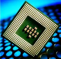
<figure class="aligncenter size-full is-resized" style="margin: 0px auto; display: table; clear: both; float: none; text-align: center;">
 <figcaption class="wp-element-caption" style="display: table-caption; margin-bottom: 1em; margin-top: 0.5em; caption-side: bottom;">Flip Chip Packaging Substrate</figcaption></figure>Fine Pitch Bumping: The demand for higher I/O density has driven the evolution of flip chip packaging substrates to support fine pitch bumping. This involves reducing the spacing between solder bumps, enabling more I/O connections within a smaller area. Fine pitch bumping advancements have facilitated the development of advanced microprocessors, graphics cards, and other high-performance integrated circuits. Applications of Flip Chip Packaging Substrates, Flip chip packaging substrates find diverse applications across various electronic devices, serving industries ranging from consumer electronics to high-end data centers. Notable applications include: Mobile Devices: The compact size, improved electrical performance, and enhanced thermal dissipation offered by flip chip packaging substrates make them ideal for mobile devices like smartphones and tablets. These substrates enable the integration of powerful processors, high-resolution displays, and advanced sensors in a small form factor.
Flip chip packaging substrates offer compactness, electrical reliability, and high-density interconnects, making them well-suited for medical applications. Conclusion Flip chip packaging substrates play a pivotal role in advancing microelectronics and the development of high-performance electronic devices. Ongoing advancements in substrate materials, interconnect technologies, and the integration of embedded passives continue to enhance the performance and reliability of flip chip packaging substrates. From mobile devices to data centers, automotive electronics to medical devices, the applications of flip chip packaging substrates are extensive and diverse. As technology continues to progress, these substrates will further push the boundaries of electronic packaging, enhancing the capabilities of our interconnected world.
If you have any problem with production process capacity or material, please contact our engineers directly. We will help you sincerely and quickly without any consulting fees. Our email: INFO@ALCANTAPCB.COM
1 Comments
Comments
friend